2-24
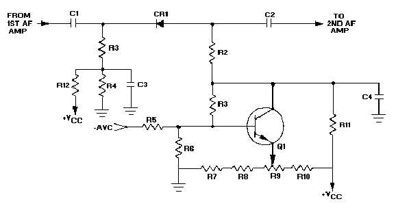
typical circuit of this type. The circuit cuts off receiver output when no input signal is being received. It
accomplishes this by blocking either the detector or audio amplifier when no signal is present. Let’s take a
look at the theory involved in this process.
Figure 2-21.—Squelch circuit.
The squelch diode CR1 connects the output of the first af stage to the input of the second. Amplifier
Q1 serves as the control transistor for the circuit. The anode and cathode voltages of CR1 are normally
biased positive with respect to ground.
With no input signal, R9 is adjusted until Q1 draws enough collector current to reduce its collector
voltage and the anode voltage of CR1 to a value below the voltage on the cathode of CR1. At this point
the anode voltage of the squelch diode is negative with respect to its cathode, and conduction ceases.
Audio output is now reduced to zero and the receiver is silent.
The base of Q1 is connected to the automatic volume control (avc) line. Anytime a signal enters the
receiver, a negative avc voltage is applied to the base of Q1. This reduces the collector current and
increases the collector voltage, which in turn increases the anode voltage of CR1 until the anode becomes
positive with respect to the cathode. Once again diode CR1 will conduct, and the signal will be passed to
the second af amplifier. Diode CR1 is effectively a switch controlled by the avc voltage.
Q19. What is a disadvantage of agc?
Q20. What is the main difference between agc and dagc?
Q21. What is the function of the bfo?
Q22. What is the purpose of a squelch circuit?


