2-19
antenna will increase to 15 microvolts. To maintain the desired 1 millivolt of output signal, you must
somehow reduce the gain of the rf amplifier. With an input of 15 microvolts and a desired output of 1
millivolt (1,000 microvolts), the gain of the amplifier must be reduced to:
When the 10-microvolt original signal and the 5-microvolt reflected signal are out of phase with each
other, the signal strength at the receiving antenna will decrease to 5 microvolts. If we want to maintain
our original 1,000-microvolt output signal, the voltage gain of the amplifier must be increased as follows:
A variation of amplifier gain, similar to the example, is necessary if we are going to compensate for
input signal strength variations. The required amplifier gain variations can be accomplished automatically
by the addition of an agc circuit within the receiver. Let’s take a look at the methods and circuits used to
produce agc and the manner in which agc (avc) controls receiver gain.
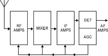
CIRCUITRY.—Figure 2-15 is a block diagram representing agc feedback to preceding stages. The
detector circuit has a dc component in the output that is directly proportional to the average amplitude of
the modulated carrier. The agc circuitry uses this dc component by filtering the detector output to remove
the audio and IF components and by applying a portion of the dc component to the preceding stages. This
agc voltage controls the amplification of any or all of the stages preceding the detector stage. Solid-state
receivers may use either positive or negative voltage for agc. The type of transistors used and the
elements to which the control voltage is applied determine which type we will have.
Figure 2-15.—Block diagram showing agc application.
The circuit shown in figure 2-16 produces a positive agc voltage. Transformer T1, diode CR1,
capacitor C1, and resistor R1 comprise a series diode detector. The agc network is made up of R2 and C2.
With normal detector operation and the positive (+) potential shown at the input, CR1 conducts.
Conduction of the diode will cause a charging current (shown by the dashed line) to flow through agc
capacitor C2 and agc resistor R2. This charging current develops a voltage across C2. When the potential
across T1 reverses, the diode will be reverse biased and will not conduct. When this happens, the charging
current ceases and C2 begins to discharge. The discharge path for C2 is shown by the solid arrows. The


