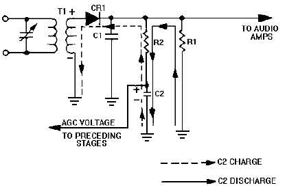
2-20
discharge path time constant of C2, R1, and R2 is chosen to be longer than the period (1/f) of the lowest
audio frequency present in the output of the detector. Because of the longer time constant, C2 will not
discharge much between peaks of the modulating signal, and the voltage across C2 will be essentially a dc
voltage. This voltage is proportional to the average signal amplitude. Now, if the signal strength varies,
C2 will either increase or decrease its charge, depending on whether the signal increases or decreases.
Since the charge on the agc capacitor responds only to changes in the average signal level, instantaneous
variations in the signal will not affect the agc voltage.
Figure 2-16.—Series diode detector and simple agc circuit.
You should remember that, depending on transistor types, the receiver may require either a positive
or a negative agc voltage. A negative agc voltage could be easily obtained by reversing CR1. Once the
values for R2 and C2 have been selected, the voltage divider action of the components is fixed, and the
circuit operates automatically without further adjustment. If the average amplitude of the signal increases,
the charge on C2 will also increase. If the signal amplitude decreases so does the charge on C2.
The agc voltages in a receiver provide controlled degenerative feedback. By adjusting the operating
point of an amplifier, you can control the gain. Under no-signal conditions, bias of the rf and IF amplifiers
is developed by standard means, such as self bias. With an applied signal, an agc voltage is developed,
which in conjunction with normal biasing methods develops the operating bias for the amplifiers.
TRANSISTOR AMPLIFIER GAIN.—You have seen how a dc voltage that is obtained at the
output of the agc network is proportional to, and will reflect, the average variations of the average signal
level. Now all we have to do is use this agc voltage to control the amplification of one or more of the
preceding amplifiers. Figure 2-17 illustrates a common-emitter amplifier with agc applied to the base
element. A change in the agc voltage will change the operating point of the transistor and the dc emitter
current. In this circuit, R1 and R4 form a voltage divider and establish no-signal (forward) bias on the
base. Since a pnp transistor is used, the base has a negative potential. The agc voltage from the detector is
positive with respect to ground and is fed to the base through dropping resistor R2. You will find when
the dc output of the detector increases (because of an increase in the average signal level) the agc voltage
will become more positive. This increased positive potential is applied to the base of Q1, which decreases
the forward bias of Q1 and decreases the gain of the amplifier. Agc, in this application, works with


