2-17
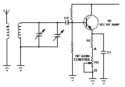
the rf gain may be reduced to prevent overloading. A typical manual gain control circuit for a receiver is
illustrated in figure 2-13. Let’s go through the basic circuitry.
Figure 2-13.—Typical rf gain control.
C1 is an emitter bypass capacitor. Resistors R1 and R2 develop emitter bias for the amplifier. C2
provides dc isolation between the tank and the base of transistor Q1. You should recall from your studies
of NEETS, Module 7, Introduction to Solid-State Devices and Power Supplies, and Module 8,
Introduction to Amplifiers, that amplifier gain may be varied by changing bias. Potentiometer R2, the rf
gain control, is nothing more than a manual bias adjustment. When the wiper arm of R2 is set at point B,
minimum forward bias is applied to the transistor. This causes the amplifier to operate closer to cutoff and
reduces gain. When you move the control toward point A, the opposite occurs. R1 limits the maximum
conduction of Q1 when R2 is short circuited. You may run into an alternate biasing method when the
transistor is operated near saturation. In that case, a large change in gain would again be a function of
bias.
Manual Volume Control (mvc)
Figure 2-14 shows the circuitry for a common method of controlling volume in a superheterodyne
receiver. C1 and R1 form an input signal coupling circuit and are also the means of controlling the level
applied to the audio amplifier. R1, R2, and R3 develop forward bias and set the operating point for the
transistor amplifier. R4 is the collector load resistor for Q1, and C3 is the output coupling capacitor.
Potentiometer R1 in the circuit shown causes the input impedance of the stage to remain fairly constant.
The signal from the preceding stage is felt across R1. By adjusting R1, you can change the input level to
Q1 and vary the output amplitude.


