4-24
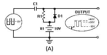
Figure 4-20A.—Positive clamper with negative bias.
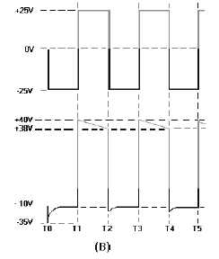
Figure 4-20B.—Positive clamper with negative bias.
The
-
25 volt input signal provides forward bias for D1. The capacitor charges to +15 volts and
retains most of its charge because its discharge through R1 is negligible. The +25 volt input signal is
series aiding the capacitor voltage and develops +40 volts between the output terminals. When the input
voltage is
-
25 volts, D1 conducts and the output voltage is
-
10 volts (
-
25 volts plus +15 volts). In this
way the output reference is clamped at
-
10 volts. Changing the size of the battery changes the clamping
reference level to the new voltage.
NEGATIVE-DIODE CLAMPERS
Figure 4-21, view (A), illustrates the circuit of a negative-diode clamper. Compare this with the
positive-diode clamper in view (A) of figure 4-18. Note that the diode is reversed with reference to
ground. Like the positive clamper, resistor R1 provides a discharge path for C1; the resistance must be a
large value for C1 to have a long discharge time. The low resistance of the diode provides a fast charge
path for C1. Once C1 becomes charged, it acts as a source of voltage which will help determine the
maximum and minimum voltage levels of the output wave shape. The input wave shape shown in view
(B) is a square wave which varies between +25 and
-
25 volts. The output wave shapes are shown in the
bottom half of view (B). You will find that the operation of the negative clamper is similar to that of the
positive clamper, except for the reversal of polarities.


