3-40
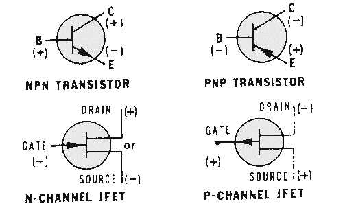
Figure 3-46.—Symbols and bias voltages for transistors and JFET.
The key to FET operation is the effective cross-sectional area of the channel, which can be controlled
by variations in the voltage applied to the gate. This is demonstrated in the figures which follow.
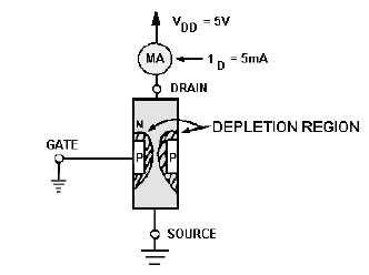
Figure 3-47 shows how the JFET operates in a zero gate bias condition. Five volts are applied across
the JFET so that current flows through the bar from source to drain, as indicated by the arrow. The gate
terminal is tied to ground. This is a zero gate bias condition. In this condition, a typical bar represents a
resistance of about 500 ohms. A milliammeter, connected in series with the drain lead and dc power,
indicates the amount of current flow. With a drain supply (VDD) of 5 volts, the milliammeter gives a drain
current (ID) reading of 10 milliamperes. The voltage and current subscript letters (V
DD, ID) used for an
FET correspond to the elements of the FET just as they do for the elements of transistors.
Figure 3-47.—JFET operation with zero gate bias.
In figure 3-48, a small reverse-bias voltage is applied to the gate of the JFET. A gate-source voltage
(VGG) of negative 1 volt applied to the P-type gate material causes the junction between the P- and N-type
material to become reverse biased. Just as it did in the varactor diode, a reverse-bias condition causes a


