3-27
The operation of the circuit to this point has generated a very steep leading edge for the output pulse.
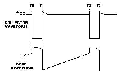
Figure 3-34 shows the idealized collector and base waveforms. Once the base of Q1 (figure 3-33)
becomes saturated, the current increase in L1 is determined by the time constant of L1 and the total series
resistance. From T0 to T1 in figure 3-34 the current increase (not shown) is approximately linear. The
voltage across L1 will be a constant value as long as the current increase through L1 is linear.
Figure 3-34.—Blocking oscillator idealized waveforms.
At time T1, L1 saturates. At this time, there is no further change in magnetic flux and no coupling
from L1 to L2. C1, which has charged during time TO to T1, will now discharge through R1 and cut off
Q1. This causes collector current to stop, and the voltage across L1 returns to 0.
The length of time between T0 and T1 (and T2 to T3 in the next cycle) is the pulse width, which
depends mainly on the characteristics of the transformer and the point at which the transformer saturates.
A transformer is chosen that will saturate at about 10 percent of the total circuit current. This ensures that
the current increase is nearly linear. The transformer controls the pulse width because it controls the slope
of collector current increase between points T0 and T1. Since TC = L ÷ R , the greater the L, the longer
the TC. The longer the time constant, the slower the rate of current increase. When the rate of current
increase is slow, the voltage across L1 is constant for a longer time. This primarily determines the pulse
width.
From T1 to T2 (figure 3-34), transistor Q1 is held at cutoff by C1 discharging through R1 (figure
3-33). The transistor is now said to be "blocked." As C1 gradually loses its charge, the voltage on the base
of Q1 returns to a forward-bias condition. At T2, the voltage on the base has become sufficiently positive
to forward bias Q1, and the cycle is repeated.
The collector waveform may have an INDUCTIVE OVERSHOOT (PARASITIC OSCILLATIONS)
at the end of the pulse. When Q1 cuts off, current through L1 ceases, and the magnetic field collapses,
inducing a positive voltage at the collector of Q1. These oscillations are not desirable, so some means
must be employed to reduce them. The transformer primary may be designed to have a high dc resistance
resulting in a low Q; this resistance will decrease the amplitude of the oscillations. However, more
damping may be necessary than such a low-Q transformer primary alone can achieve. If so, a DAMPING
resistor can be placed in parallel with L1, as shown in figure 3-35.