3-36
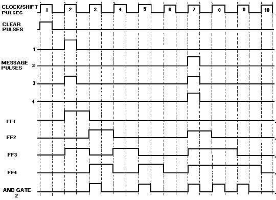
Figure 3-32. —Parallel-to-serial conversion timing diagram.
At CP1, a CLEAR pulse is applied to all the FFs, resetting the register to a count of 0. The number
01012 is applied to the parallel inputs at CP2, causing FF1 and FF3 to set. At this point, the J inputs of
FF2 and FF4 are HIGH. AND gate 2 has a LOW output since the FF4 output is LOW. This LOW output
represents the first digit of the number 01012 to be output in serial form. At the same time we have
HIGHs on the K inputs of FF1 and FF3. (Notice the NOT symbol on FF1 at input K. With no serial input
to AND gate 1, the output is LOW; therefore, the K input to FF1 is held HIGH). With these conditions
CP3 causes FF1 and FF3 to reset and FF2 and FF4 to set. The HIGH output of FF4, along with CP3,
causes AND gate 2 to output a HIGH. This represents the second digit of the number 01012.
At CP4, FF2 and FF4 reset, and FF3 sets. FF1 remains reset because of the HIGH at the K input. The
output of AND gate 2 goes LOW because the output of FF4 is LOW and the third digit of the number is
output on the serial line. CP5 causes FF4 to set and FF3 to reset. CP5 and the HIGH from FF4 cause
AND gate 2 to output the last digit of the number on the serial line. It took a total of four CLK pulses to
input the number in parallel and output it in serial.
CP6 causes FF4 to reset and effectively clears the register for the next parallel input.
Between CP7 and CP10, the number 11102 is input as parallel data and output as serial data.
Serial-to-Parallel Conversion
Serial input is accomplished much in the same manner as serial output. Instead of shifting the data
out one bit at a time, we shift the data in one bit at a time.
To understand this conversion, you should again use figure 3-31and also the timing diagram shown
in figure 3-33. In this example we will convert the number 10112 from serial data to parallel data.


