3-6
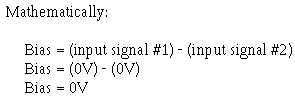
In figure 3-3 at time zero (T0) both input signals are at 0 volts. The output signal is also at 0 volts.
Between time zero (T0) and time one (T1), input signal number one goes positive and input signal
number two goes negative. Each of these voltage changes causes an increase in the base-to-emitter bias
which causes current through Q1 to increase. Increased current through Q1 results in a greater voltage
drop across the collector load (R3) which causes the output signal to go negative.
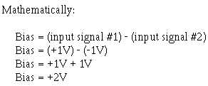
By time one (T1), input signal number one has reached +1 volt and input signal number two has
reached -1 volt. This is an overall increase in base-to-emitter bias of 2 volts. Since the gain of the circuit
is -10, the output signal has decreased by 20 volts. As you can see, the output signal has been determined
by the difference between the two input signals. In fact, the base-to-emitter bias can be found by
subtracting the value of input signal number two from the value of input signal number one.
Between time one (T1) and time two (T2), input signal number one goes from +1 volt to 0 volts and
input signal number two goes from -1 volt to 0 volts. At time two (T2) both input signals are at 0 volts
and the base-to-emitter bias has returned to 0 volts. The output signal is also 0 volts.
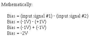
Between time two (T2) and time three (T3), input signal number one goes negative and input signal
number two goes positive. At time three (T3), the value of the base-to-emitter bias is -2 volts.
This causes the output signal to be +20 volts at time three (T3).
Between time three (T3) and time four (T4), input signal #1 goes from -1 volt to 0 volts and input
signal #2 goes from +1 volt to 0 volts. At time four (T4) both input signals are 0 volts, the bias is 0 volts,
and the output is 0 volts.
During time four (T4) through time eight (T8), the circuit repeats the sequence of events that took
place from time zero (T0) through time four (T4).

