4-43
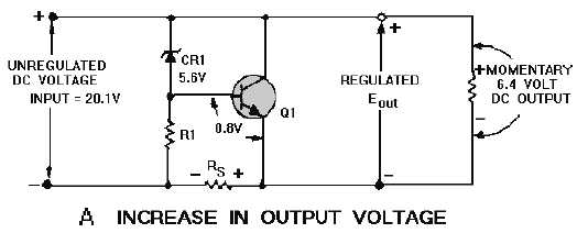
Now, refer to view A of figure 4-39. This figure shows the schematic diagram of the same shunt
voltage regulator as that shown in figure 4-38 with an increased input voltage of 20.1 volts. This increases
the forward bias on Q1 to 0.8 volt. Recall that the voltage drop across CR1 remains constant at 5.6 volts.
Since the output voltage is composed of the Zener voltage and the base-emitter voltage, the output voltage
momentarily increases to 6.4 volts. At this time, the increase in the forward bias of Q1 lowers the
resistance of the transistor allowing more current to flow through it. Since this current must also pass
through RS, there is also an increase in the voltage drop across this resistor. The voltage drop across RS is
now 13.8 volts and therefore the output voltage is reduced to 6.3 volts. Remember, this change takes
place in a fraction of a second.
Figure 4-39A.—Shunt voltage regulator. INCREASE IN OUTPUT VOLTAGE
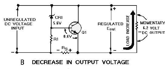
Study the schematic shown in view B. Although this schematic is identical to the other shunt voltage
schematics previously illustrated and discussed, the output voltage is different. The load current has
increased causing a momentary drop in voltage output to 6.2 volts. Recall that the circuit was designed to
ensure a constant output voltage of 6.3 volts. Since the output voltage is less than that required, changes
occur in the regulator to restore the output to 6.3 volts. Because of the 0.1 volt drop in the output voltage,
the forward bias of Q1 is now 0.6 volt. This decrease in the forward bias increases the resistance of the
transistor, thereby reducing the current flow through Q1 by the same amount that the load current
increased. The current flow through RS returns to its normal value and restores the output voltage to 6.3
volts.
Figure 4-39B.—Shunt voltage regulator. DECREASE IN OUTPUT VOLTAGE


