3-12
smaller. As the overlap between the two energy bands becomes smaller, fewer and fewer electrons can
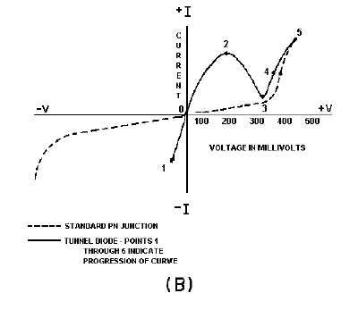
tunnel across the junction. The portion of the curve between point 2 and point 3 in which current
decreases as the voltage increases is the negative resistance region of the tunnel diode.
Figure 3-8A.—Tunnel diode energy diagram with 450 millivolts bias.
Figure 3-8B.—Tunnel diode energy diagram with 450 millivolts bias.
Figure 3-9, view A, is the energy diagram of a tunnel diode in which the forward bias has been
increased even further. The energy bands no longer overlap and the diode operates in the same manner as
a normal PN junction, as shown by the portion of the curve in view (B) from point 3 to point 4.


