3-10
Figure 3-6B.—Tunnel diode energy diagram with no bias.
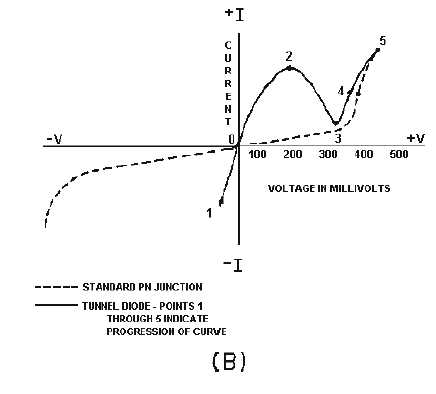
Figure 3-7, view A, shows the energy diagram of a tunnel diode with a small forward bias (50
millivolts) applied. The bias causes unequal energy levels between some of the majority carriers at the
energy band overlap point, but not enough of a potential difference to cause the carriers to cross the
forbidden gap in the normal manner. Since the valence band of the P-material and the conduction band of
the N-material still overlap, current carriers tunnel across at the overlap and cause a substantial current
flow. The amount of current flow is marked by point 2 on the curve in view B. Note in view A that the
amount of overlap between the valence band and the conduction band decreased when forward bias was
applied.

