3-9
the depletion region is only one-millionth of an inch. You might think of the process simply as an arc-
over between the N- and the P-side across the depletion region.
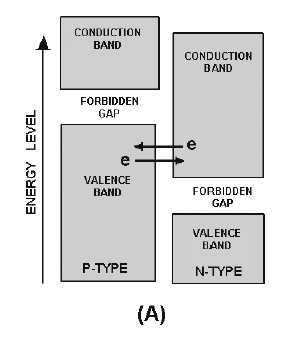
Figure 3-6 shows the equilibrium energy level diagram of a tunnel diode with no bias applied. Note
in view A that the valence band of the P-material overlaps the conduction band of the N-material. The
majority electrons and holes are at the same energy level in the equilibrium state. If there is any
movement of current carriers across the depletion region due to thermal energy, the net current flow will
be zero because equal numbers of current carriers flow in opposite directions. The zero net current flow is
marked by a "0" on the current-voltage curve illustrated in view B.
Figure 3-6A.—Tunnel diode energy diagram with no bias.

