1-11
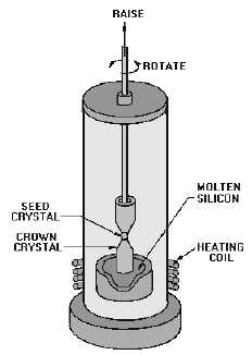
Figure 1-9.—Crystal furnace.
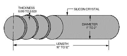
The cylinder of semiconductor material that is grown is sliced into thicknesses of .010 to .020 inch in
the first step of preparation, as shown in figure 1-10. These wafers are ground and polished to remove any
irregularities and to provide the smoothest surface possible. Although both sides are polished, only the
side that will receive the components must have a perfect finish.
Figure 1-10.—Silicon crystal and wafers.
Q17. What are the basic steps in manufacturing an IC?
Q18. Computer-aided layout is used to prepare _______ devices.
Q19. What purpose do masks serve?
Q20. What type of substrates are used for film and hybrid ICs?


