1-10
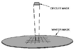
Figure 1-8.—Wafer mask distribution.
A wafer mask is a device used to deposit materials on a substrate. It allows material to be deposited
in certain areas, but not in others. By changing the pattern of the mask, we can change the component
arrangement of the circuit. Several different masks may be used to produce a simple microelectronic
device. When used in proper sequence, conductor, semiconductor, or insulator materials may be applied
to the substrate to form transistors, resistors, capacitors, and interconnecting leads.
SUBSTRATE PRODUCTION
As was mentioned earlier in this topic, microelectronic devices are produced on a substrate. This
substrate will be of either insulator or semiconductor material, depending on the type of device. Film and
hybrid ICs are normally constructed on a glass or ceramic substrate. Ceramic is usually the preferred
material because of its durability.
Substrates used in monolithic ICs are of semiconductor material, usually silicon. In this type of IC,
the substrate can be an active part of the IC. Glass or ceramic substrates are used only to provide support
for the components.
Semiconductor substrates are produced by ARTIFICIALLY GROWING cylindrical CRYSTALS of
pure silicon or germanium. Crystals are "grown" on a SEED CRYSTAL from molten material by slowly
lifting and cooling the material repeatedly. This process takes place under rigidly controlled atmospheric
and temperature conditions.
Figure 1-9 shows a typical CRYSTAL FURNACE. The seed crystal is lowered until it comes in
contact with the molten material-silicon in this case. It is then rotated and raised very slowly. The seed
crystal is at a lower temperature than the molten material. When the molten material is in contact with the
seed, it solidifies around the seed as the seed is lifted. This process continues until the grown crystal is of
the desired length. A typical crystal is about 2 inches in diameter and 10 to 12 inches long. Larger
diameter crystals can be grown to meet the needs of the industry. The purity of the material is strictly
controlled to maintain specific semiconductor properties. Depending on the need, n or p impurities are
added to produce the desired characteristics. Several other methods of growing crystals exist, but the
basic concept of crystal production is the same.


