1-13
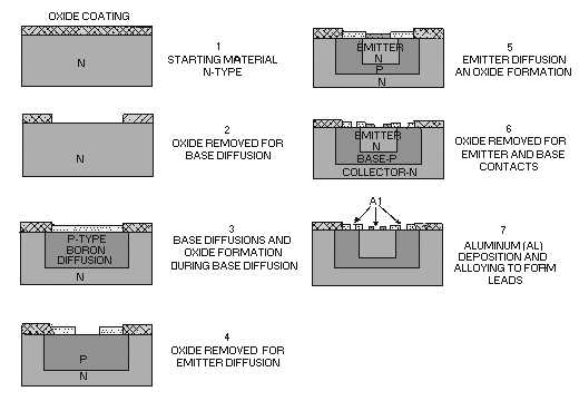
Figure 1-12.—Planar-diffused transistor.
1. An oxide coating is thermally grown over the n-type silicon starting material.
2. By means of the photolithographic process, a window is opened through the oxide layer. This is
done through the use of masks, as discussed earlier.
3. The base of the transistor is formed by placing the wafer in a diffusion furnace containing a p-
type impurity, such as boron. By controlling the temperature of the oven and the length of time
that the wafer is in the oven, you can control the amount of boron diffused through the window
(the boron will actually spread slightly beyond the window opening). A new oxide layer is then
allowed to form over the area exposed by the window.
4. A new window, using a different mask much smaller than the first, is opened through the new
oxide layer.
5. An n-type impurity, such as phosphorous, is diffused through the new window to form the
emitter portion of the transistor. Again, the diffused material will spread slightly beyond the
window opening. Still another oxide layer is then allowed to form over the window.
6. By means of precision-masking techniques, very small windows (about 0.005 inch in diameter)
are opened in both the base and emitter regions of the transistor to provide access for electrical
currents.
7. Aluminum is then deposited in these windows and alloyed to form the leads of the transistor or
the IC.
(Note that the pn junctions are covered throughout the fabrication process by an oxide layer that
prevents contamination.)


