1-24
used to encapsulate the IC die, no void will exist between the cover and die, as is the case with ceramic
packaging.
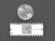
At present, ceramic DIPs are the most common of the two package types to be found in Navy
microelectronic systems. Figure 1-25 shows a DIP which has been opened.
Figure 1-25.—Dual inline package (DIP).
RECENT DEVELOPMENTS IN PACKAGING
Considerable effort has been devoted to eliminating the fine wires used to connect ICs to Kovar
leads. The omission of these wires reduces the cost of integrated circuits by eliminating the costs
associated with the bonding process. Further, omission of the wires improves reliability by eliminating a
common cause of circuit failure.
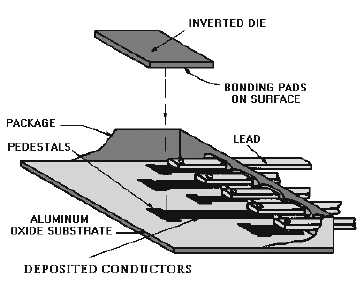
A promising packaging technique is the face-down (FLIP-CHIP) mounting method by which
conductive patterns are evaporated inside the package before the die is attached. These patterns connect
the external leads to bonding pads on the inside surface of the die. The pads are then bonded to
appropriate pedestals on the package that correspond to those of the bonding pads on the die (figure 1-26).
Figure 1-26.—Flip-chip package.
The BEAM-LEAD technique is a process developed to batch-fabricate (fabricate many at once)
semiconductor circuit elements and integrated circuits with electrodes extended beyond the edges of the


