2-19
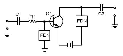
Figure 2-12.—Semiblock diagram of rf amplifier.
In this "semi-block" diagram, C1 and C2 are the input and output coupling capacitors. R1 represents
the impedance of the input circuit. The blocks marked FDN represent the frequency-determining
networks. They are used as input-signal-developing and output impedances for Q1.
FREQUENCY-DETERMINING NETWORK FOR AN RF AMPLIFIER
What kind of circuit would act as a frequency-determining network? In general, a frequency-
determining network is a circuit that provides the desired response at a particular frequency. This
response could be maximum impedance or minimum impedance; it all depends on how the frequency-
determining network is used. You will see more about frequency-determining networks in NEETS,
Module 9—Introduction to Wave-Generation and Shaping Circuits. As you have seen, the frequency-
determining network needed for an rf amplifier should have maximum impedance at the desired
frequency.
Before you are shown the actual components that make up the frequency-determining network for an
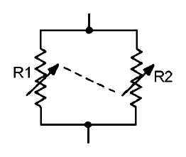
rf amplifier, look at figure 2-13, which is a simple parallel circuit. The resistors in this circuit are variable
and are connected together (ganged) in such a way that as the resistance of R1 increases, the resistance of
R2 decreases, and vice versa.
Figure 2-13.—Parallel variable resistors (ganged).
If each resistor has a range from 0 to 200 ohms, the following relationship will exist between the
individual resistances and the resistance of the network (RT). (All values are in ohms, RT rounded off to
two decimal places. These are selected values; there are an infinite number of possible combinations.)


