2-18
Before you study the specific techniques used in rf amplifiers, you should review some information
on the relationship between the input and output impedance of an amplifier and the gain of the amplifier
stage.
AMPLIFIER INPUT/OUTPUT IMPEDANCE AND GAIN
You should remember that the gain of a stage is calculated by using the input and output signals. The
formula used to calculate the gain of a stage is:
Voltage gain is calculated using input and output voltage; current gain uses input and output current;
and power gain uses input and output power. For the purposes of our discussion, we will only be
concerned with voltage gain.
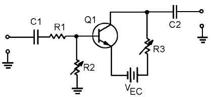
Figure 2-11 shows a simple amplifier circuit with the input- and output-signal-developing
impedances represented by variable resistors. In this circuit, C1 and C2 are the input and output coupling
capacitors. R1 represents the impedance of the input circuit. R2 represents the input-signal-developing
impedance, and R3 represents the output impedance.
Figure 2-11.—Variable input and output impedances.
R1 and R2 form a voltage-divider network for the input signal. When R2 is increased in value, the
input signal to the transistor (Q1) increases. This causes a larger output signal, and the gain of the stage
increases.
Now look at the output resistor, R3. As R3 is increased in value, the output signal increases. This
also increases the gain of the stage.
As you can see, increasing the input-signal-developing impedance, the output impedance, or both
will increase the gain of the stage. Of course there are limits to this process. The transistor must not be
overdriven with too high an input signal or distortion will result.
With this principle in mind, if you could design a circuit that had maximum impedance at a specific
frequency (or band of frequencies), that circuit could be used in an rf amplifier. This FREQUENCY-
DETERMINING NETWORK could be used as the input-signal-developing impedance, the output
impedance, or both. The rf amplifier circuit would then be as shown in figure 2-12.


