3-3
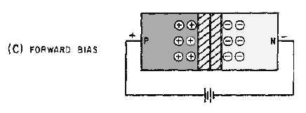
Figure 3-1C.—Effects of bias on the depletion region of a PN junction.
There are two distinct theories used to explain the behavior of PN junctions during breakdown: one
is the ZENER EFFECT and the other is the AVALANCHE EFFECT.
The ZENER EFFECT was first proposed by Dr. Carl Zener in 1934. According to Dr. Zener's
theory, electrical breakdown in solid dielectrics occurs by a process called QUANTUM-MECHANICAL
TUNNELING. The Zener effect accounts for the breakdown below 5 volts; whereas, above 5 volts the
breakdown is caused by the avalanche effect. Although the avalanche effect is now accepted as an
explanation of diode breakdown, the term Zener diode is used to cover both types.
The true Zener effect in semiconductors can be described in terms of energy bands; however, only
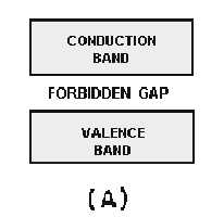
the two upper energy bands are of interest. The two upper bands, illustrated in figure 3-2, view A, are
called the conduction band and the valence band.
Figure 3-2A.-Energy diagram for Zener diode.
The CONDUCTION BAND is a band in which the energy level of the electrons is high enough that
the electrons will move easily under the influence of an external field. Since current flow is the movement
of electrons, the readily mobile electrons in the conduction band are capable of maintaining a current flow
when an external field in the form of a voltage is applied. Therefore, solid materials that have many
electrons in the conduction band are called conductors.
The VALENCE BAND is a band in which the energy level is the same as the valence electrons of
the atoms. Since the electrons in these levels are attached to the atoms, the electrons are not free to move
around as are the conduction band electrons. With the proper amount of energy added, however, the
electrons in the valence band may be elevated to the conduction band energy level. To do this, the
electrons must cross a gap that exists between the valence band energy level and the conduction band
energy level. This gap is known as the FORBIDDEN ENERGY BAND or FORBIDDEN GAP. The


