1-14
EPITAXIAL METHOD.—The EPITAXIAL process involves depositing a very thin layer of
silicon to form a uniformly doped crystalline region (epitaxial layer) on the substrate. Components are
produced by diffusing appropriate materials into the epitaxial layer in the same way as the planar-
diffusion method. When planar-diffusion and epitaxial techniques are combined, the component
characteristics are improved because of the uniformity of doping in the epitaxial layer. A cross section of
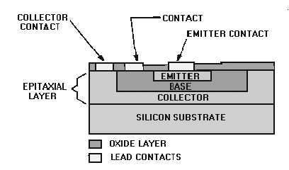
a typical planar-epitaxial transistor is shown in figure 1-13. Note that the component parts do not
penetrate the substrate as they did in the planar-diffused transistor.
Figure 1-13.—Planar-epitaxial transistor.
ISOLATION.—Because of the closeness of components in ICs, ISOLATION from each other
becomes a very important factor. Isolation is the prevention of unwanted interaction or leakage between
components. This leakage could cause improper operation of a circuit.
Techniques are being developed to improve isolation. The most prominent is the use of silicon oxide,
which is an excellent insulator. Some manufacturers are experimenting with single-crystal silicon grown
on an insulating substrate. Other processes are also used which are far too complex to go into here. With
progress in isolation techniques, the reliability and efficiency of ICs will increase rapidly.
Thin Film
Thin film is the term used to describe a technique for depositing passive circuit elements on an
insulating substrate with coating to a thickness of 0.0001 centimeter. Many methods of thin-film
deposition exist, but two of the most widely used are VACUUM EVAPORATION and CATHODE
SPUTTERING.
VACUUM EVAPORATION.—Vacuum evaporation is a method used to deposit many types of
materials in a highly evacuated chamber in which the material is heated by electricity, as shown in figure
1-14. The material is radiated in straight lines in all directions from the source and is shadowed by any
objects in its path.