1-9
Development of a microelectronic device begins with a demand from industry or as the result of
research. A device that is needed by industry may be a simple diode network or a complex circuit
consisting of thousands of components. No matter how complex the device, the basic steps of production
are similar. Each type of device requires circuit design, component arrangement, preparation of a
substrate, and the depositing of proper materials on the substrate.
The first consideration in the development of a new device is to determine what the device is to
accomplish. Once this has been decided, engineers can design the device. During the design phase, the
engineers will determine the numbers and types of components and the interconnections, needed to
complete the planned circuit.
COMPONENT ARRANGEMENT
Planning the component arrangement for a microelectronic device is a very critical phase of
production. Care must be taken to ensure the most efficient use of space available. With simple devices,
this can be accomplished by hand. In other words, the engineers can prepare drawings of component
placement. However, a computer is used to prepare the layout for complex devices. The computer is able
to store the characteristics of thousands of components and can provide a printout of the most efficient
component placement. Component placement is then transferred to extremely large drawings. During this
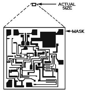
step, care is taken to maintain the patterns as they will appear on the substrate. Figure 1-7 shows a fairly
simple IC MASK PATTERN. If this pattern were being prepared for production, it would be drawn
several hundred times the size shown and then photographed. The photo would then be reduced in size
until it was the actual desired size. At that time, the pattern would be used to produce several hundred
patterns that would be used on one substrate. Figure 1-8 illustrates how the patterns would be distributed
to act as a WAFER MASK for manufacturing.
Figure 1-7.—IC mask pattern.


