1-15
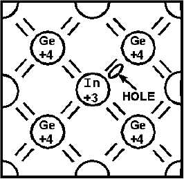
electron short of the required amount of electrons needed to form covalent bonds with 4 neighboring
atoms and, therefore, creates a hole in the structure. Gallium and boron, which are also trivalent
impurities, exhibit these same characteristics when added to germanium. The holes can only be present in
this type semiconductor when a trivalent impurity is used. Note that a hole carrier is not created by the
removal of an electron from a neutral atom, but is created when a trivalent impurity enters into covalent
bonds with a tetravalent (4 valence electrons) crystal structure. The holes in this type of semiconductor
(P-type) are considered the MAJORITY carriers since they are present in the material in the greatest
quantity. The electrons, on the other hand, are the MINORITY carriers.
Figure 1-11.—Germanium crystal doped with indium.
Q17. What is the name given to a doped germanium crystal with an excess of free holes?
Q18. What are the majority carriers in an N-type semiconductor?
SEMICONDUCTOR DIODE
If we join a section of N-type semiconductor material with a similar section of P-type semiconductor
material, we obtain a device known as a PN JUNCTION. (The area where the N and P regions meet is
appropriately called the junction.) The usual characteristics of this device make it extremely useful in
electronics as a diode rectifier. The diode rectifier or PN junction diode performs the same function as its
counterpart in electron tubes but in a different way. The diode is nothing more than a two-element
semiconductor device that makes use of the rectifying properties of a PN junction to convert alternating
current into direct current by permitting current flow in only one direction. The schematic symbol of a PN
junction diode is shown in figure 1-12. The vertical bar represents the cathode (N-type material) since it is
the source of electrons and the arrow represents the anode. (P-type material) since it is the destination of
the electrons. The label "CR1" is an alphanumerical code used to identify the diode. In this figure, we
have only one diode so it is labeled CR1 (crystal rectifier number one). If there were four diodes shown in
the diagram, the last diode would be labeled CR4. The heavy dark line shows electron flow. Notice it is
against the arrow. For further clarification, a pictorial diagram of a PN junction and an actual
semiconductor (one of many types) are also illustrated.