1-13
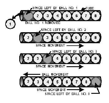
Figure 1-9.—Analogy of hole flow.
When ball number 1 is removed from the tube, a hole is left. This hole is then filled by ball number
2, which leaves still another hole. Ball number 3 then moves into the hole left by ball number 2. This
causes still another hole to appear where ball 3 was. Notice the holes are moving to the right side of the
tube. This action continues until all the balls have moved one space to the left in which time the hole
moved eight spaces to the right and came to rest at the right-hand end of the tube.
In the theory just described, two current carriers were created by the breaking of covalent bonds: the
negative electron and the positive hole. These carriers are referred to as electron-hole pairs. Since the
semiconductor we have been discussing contains no impurities, the number of holes in the electron-hole
pairs is always equal to the number of conduction electrons. Another way of describing this condition
where no impurities exist is by saying the semiconductor is INTRINSIC. The term intrinsic is also used to
distinguish the pure semiconductor that we have been working with from one containing impurities.
Q15. Name the two types of current flow in a semiconductor.
Q16. What is the name given to a piece of pure semiconductor material that has an equal number of
electrons and holes?
DOPING PROCESS
The pure semiconductor mentioned earlier is basically neutral. It contains no free electrons in its
conduction bands. Even with the application of thermal energy, only a few covalent bonds are broken,
yielding a relatively small current flow. A much more efficient method of increasing current flow in
semiconductors is by adding very small amounts of selected additives to them, generally no more than a
few parts per million. These additives are called impurities and the process of adding them to crystals is
referred to as DOPING. The purpose of semiconductor doping is to increase the number of free charges
that can be moved by an external applied voltage. When an impurity increases the number of free
electrons, the doped semiconductor is NEGATIVE or N TYPE, and the impurity that is added is known
as an N-type impurity. However, an impurity that reduces the number of free electrons, causing more