1-19
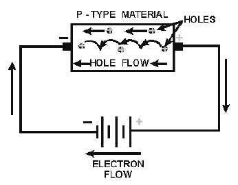
Figure 1-16.—Current flow In the P-type material.
Notice in both N-type and P-type materials, current flow in the external circuit consists of electrons
moving out of the negative terminal of the battery and into the positive terminal of the battery. Hole flow,
on the other hand, only exists within the material itself.
Q22. What are the majority carriers in a P-type semiconductor?
Q23. Conduction in which type of semiconductor material is similar to conduction in a copper wire?
Junction Barrier
Although the N-type material has an excess of free electrons, it is still electrically neutral. This is
because the donor atoms in the N material were left with positive charges after free electrons became
available by covalent bonding (the protons outnumbered the electrons). Therefore, for every free electron
in the N material, there is a corresponding positively charge atom to balance it. The end result is that the
N material has an overall charge of zero.
By the same reasoning, the P-type material is also electrically neutral because the excess of holes in
this material is exactly balanced by the number of electrons. Keep in mind that the holes and electrons are
still free to move in the material because they are only loosely bound to their parent atoms.
It would seem that if we joined the N and P materials together by one of the processes mentioned
earlier, all the holes and electrons would pair up. On the contrary, this does not happen. Instead the
electrons in the N material diffuse (move or spread out) across the junction into the P material and fill
some of the holes. At the same time, the holes in the P material diffuse across the junction into the N
material and are filled by N material electrons. This process, called JUNCTION RECOMBINATION,
reduces the number of free electrons and holes in the vicinity of the junction. Because there is a depletion,
or lack of free electrons and holes in this area, it is known as the DEPLETION REGION.
The loss of an electron from the N-type material created a positive ion in the N material, while the
loss of a hole from the P material created a negative ion in that material. These ions are fixed in place in
the crystal lattice structure and cannot move. Thus, they make up a layer of fixed charges on the two sides
of the junction as shown in figure 1-17. On the N side of the junction, there is a layer of positively
charged ions; on the P side of the junction, there is a layer of negatively charged ions. An electrostatic
field, represented by a small battery in the figure, is established across the junction between the oppositely