18
2-52. To ensure a good mechanical bond
between the board and replacement pad
and to provide good electrical contact for
components, which of the following
procedures is used?
1. Epoxying the pad to the run
2. Electroplating the repair area
3. Installing an eyelet in the pad
4. Lap-flow soldering the repair area
2-53. Breaks, holes, and cracks in pcbs are
repaired by using a mixture of
1. fiberglass and rosin
2. epoxy and powdered carbon
3. conformal coating and RTV
4. epoxy and powdered fiberglass
2-54. What is the first step in the repair of
burned or scorched boards?
1. Filling the burned area with epoxy and
fiberglass
2. Removing all discolored material
3. Removing all delaminated conductors
4. Cleaning all surfaces with solvent
2-55. Which of the following statements is
correct concerning the repair of repairable
delaminated conductors?
1. All delaminations are removed
2. Repairable delaminations are not
removed
3. All delaminations are epoxied to the
board
4. All delaminations are replaced with
insulated wire
2-56. Damage to some electronic components
can occur at what minimum electrostatic
potential?
1. 14 volts
2. 35 volts
3. 350 volts
4. 3,500 volts
2-57. Electrostatic discharge (ESD) has the
greatest effect on which of the following
devices?
1. Silicon diodes
2. Selenium rectifiers
3. Germanium transistors
4. Metal-oxide transistor
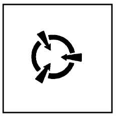
Figure 2C.
Symbol.
IN ANSWERING QUESTION 2-58, REFER TO
FIGURE 2C.
2-58. The symbol shown in the figure is found
on a component package. What does it
indicate about the component?
1. It is a high cost item
2. It is a bipolar device
3. It is an integrated circuit
4. It is electrostatic discharge sensitive
2-59. Electrostatic charges may develop as high
as which of the following voltages?
1. 3,000 volts
2. 15,000 volts
3. 20,000 volts
4. 35,000 volts


