2-18
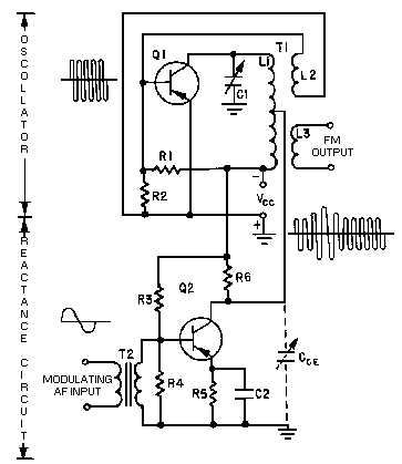
Figure 2-12.—Reactance-semiconductor fm modulator.
When the modulating signal is applied to the base of Q2, the emitter-to-base bias varies at the
modulation rate. This causes the collector voltage of Q2 to vary at the same modulating rate. When the
collector voltage increases, output capacitance CCE decreases; when the collector voltage decreases, CCE
increases. An increase in collector voltage has the effect of spreading the plates of CCE farther apart by
increasing the width of the barrier. A decrease of collector voltage reduces the width of the pn junction
and has the same effect as pushing the capacitor plates together to provide more capacitance.
When the output capacitance decreases, the instantaneous frequency of the oscillator tank circuit
increases (acts the same as if C1 were decreased). When the output capacitance increases, the
instantaneous frequency of the oscillator tank circuit decreases. This decrease in frequency produces a
lower frequency in the output because of the shunting effect of CCE. Thus, the frequency of the oscillator
tank circuit increases and decreases at an audio frequency (af) modulating rate. The output of the
oscillator, therefore, is a frequency modulated rf signal.
Since the audio modulation causes the collector voltage to increase and decrease, an AM component
is induced into the output. This produces both an fm and AM output. The amplitude variations are then
removed by placing a limiter stage after the reactance modulator and only the frequency modulation
remains.
Frequency multipliers or mixers (discussed in chapter 1) are used to increase the oscillator frequency
to the desired output frequency. For high-power applications, linear rf amplifiers are used to increase the
steady-amplitude signal to a higher power output. With the initial modulation occurring at low levels, fm
represents a savings of power when compared to conventional AM. This is because fm noise-reducing
properties provide a better signal-to-noise ratio than is possible with AM.


