2-58
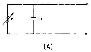
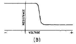
circuit of a pin diode at microwave frequencies is shown in figure 2-53A. A resistance versus voltage
characteristic curve is shown in figure 2-53B.
Figure 2-53A.—Diode equivalent circuit (pin).
Figure 2-53B.—Diode equivalent circuit (pin).
When the bias on a pin diode is varied, the microwave resistance changes from a typical value of 6
kilohms under negative bias to about 5 ohms when the bias is positive. Thus when the diode is mounted
across a transmission line or waveguide, the loading effect is insignificant while the diode is reverse
biased, and the diode presents no interference to power flow. When the diode is forward biased, the
resistance drops to approximately 5 ohms and most power is reflected. In other words, the diode acts as a
switch when mounted in parallel with a transmission line or waveguide. Several diodes in parallel can
switch power in excess of 150 kilowatts peak. The upper power limit is determined by the ability of the
diode to dissipate power. The upper frequency limit is determined by the shunt capacitance of the pn
junction, shown as C1 in figure 2-53A. Pin diodes with upper limit frequencies in excess of 30 gigahertz
are available.
Q-70. During the manufacture of a point-contact diode, what is the purpose of passing a relatively
large current from the catwhisker to the silicon crystal?
Q-71. What is the capacitive reactance across a point-contact diode as compared to a normal junction
diode?
Q-72. What are the most important advantages of the Schottky barrier diode?


