2-52
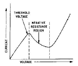
Figure 2-48.—Characteristic curve for a bulk-effect semiconductor.
If an increase in voltage is applied to a gallium-arsenide semiconductor, which is biased to operate in
the negative-resistance region, it divides into regions of varying electric fields. A tiny region, known as a
DOMAIN, forms that has an electric field of much greater intensity than the fields in the rest of the
semiconductor. The applied voltage causes the domain to travel across the semiconductor chip from the
cathode to the anode. The high field intensity of the domain is caused by the interaction of the slow
electrons in the high-energy band and the faster electrons in the low-energy band. The electrons in the
low-energy band travel faster than the moving domain and continually catch up during the transit from
cathode to anode. When the fast electrons catch up to the domain, the high field intensity forces them into
the higher band where they lose most of their mobility. This also causes them to fall behind the moving
domain. Random scattering causes the electrons to lose some energy and drop back into the lower, faster,
energy band and race again after the moving domain. The movement from the low-energy band to the
high-energy band causes the electrons to bunch up at the back of the domain and to provide the electron-
transfer energy that creates the high field intensity in the domain.
The domains form at or near the cathode and move across the semiconductor to the anode, as shown
in figure 2-49. As the domain disappears at the anode, a new domain forms near the cathode and repeats
the process.


