1-43
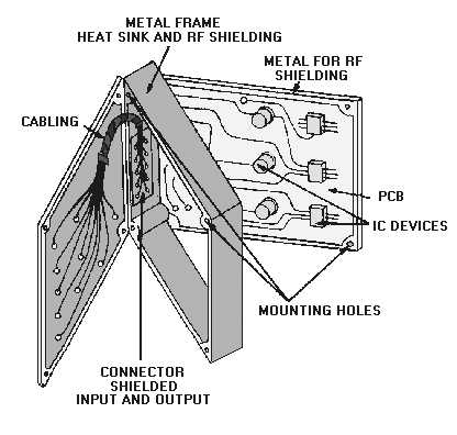
are shown in figure 1-44. As shown in the figure, rf shielding is used on the mating surfaces of the
package, cabling is shielded, and heat sinks are provided.
Figure 1-44.—Ground planes and shielding.
Interconnection and Intraconnections
To meet the high-frequency characteristics and propagation timing required by present and future
systems, the device package must not have excessive distributed capacitance and/or inductance. This type
of packaging is accomplished in the design of systems using ICs and other microelectronic devices by
using shorter leads internal to the package and by careful spacing of complex circuits on printed circuit
boards. To take advantage of the inherent speed of the integrated circuit, you must keep the signal
propagation time between circuits to a minimum. The signal is delayed approximately 1 nanosecond per
foot, so reducing the distance between circuits as much as possible is necessary. This requires the use of
structures, such as high-density digital systems with an emphasis on large-scale integration, for systems in
the future. Also, maintenance personnel should be especially concerned with the spacing of circuits, lead
dress, and surface cleanliness. These factors affect the performance of high-speed digital and analog
circuits.
Q47. In what publication are environmental requirements for equipment defined?
Q48. In what publication would you find guidelines for performance of military electronic parts?
Q49. Who is responsible for meeting environmental and electrical requirements of a system?
Q50. What methods are used to prevent unwanted component interaction?