1-7
FILM INTEGRATED CIRCUITS are broken down into two categories, THIN FILM and THICK
FILM. Film components are made of either conductive or nonconductive material that is deposited in
desired patterns on a ceramic or glass substrate. Film can only be used as passive circuit components,
such as resistors and capacitors. Transistors and/or diodes are added to the substrate to complete the
circuit. Differences in thin and thick film will be discussed later in this topic.
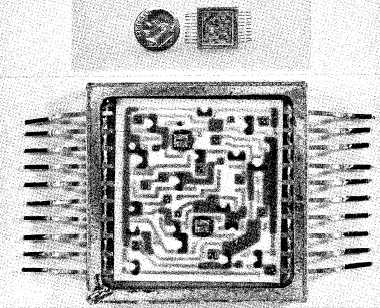
HYBRID INTEGRATED CIRCUITS combine two or more integrated circuit types or combine one
or more integrated circuit types and DISCRETE (separate) components. Figure 1-5 is an example of a
hybrid integrated circuit consisting of silicon chips and film circuitry. The two small squares are chips
and the irregularly shaped gray areas are film components.
Figure 1-5.—Hybrid integrated circuit.
STATE-OF-THE-ART MICROELECTRONICS.
Microelectronic technology today includes thin film, thick film, hybrid, and integrated circuits and
combinations of these. Such circuits are applied in DIGITAL, SWITCHING, and LINEAR (analog)
circuits. Because of the current trend of producing a number of circuits on a single chip, you may look for
further increases in the packaging density of electronic circuits. At the same time you may expect a
reduction in the size, weight, and number of connections in individual systems. Improvements in
reliability and system capability are also to be expected.
Thus, even as existing capabilities are being improved, new areas of microelectronic use are being
explored. To predict where all this use of technology will lead is impossible. However, as the demand for
increasingly effective electronic systems continues, improvements will continue to be made in state-of-
the-art microelectronics to meet the demands.
LARGE-SCALE INTEGRATION (lsi) and VERY LARGE-SCALE INTEGRATION (vlsi) are the
results of improvements in microelectronics production technology. Figure 1-6 is representative of lsi. As
shown in the figure, the entire SUBSTRATE WAFER (slice of semiconductor or insulator material) is