21
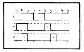
Figure 3C. OR gate timing diagram.
IN ANSWERING QUESTIONS 3-19
THROUGH 3-21, REFER TO FIGURE 3C.
3-19. The gate will have a HIGH output at
which of the following times?
1. T0 to T3, T4 to T7, and T8 to T9
2. T1 to T2 and T4 to T9
3. T3 to T4 and T7 to T8
4. T1 to T2 only
3-20. What are the input logic states between T5
and T6?
1. X = 1, Y = 0, Z = 0
2. X = 1, Y = 0, Z = 1
3. X = 0, Y = 1, Z = 0
4. X = 0, Y = 1, Z = 1
3-21. Between T0 and T6, at what times will the
output of the gate be LOW?
1. T3 to T4
2. T2 to T5
3. T3 to T6
4. T0 to T1
3-22. What is the Boolean expression for an OR
gate having the following inputs?
T (LOW)
R (LOW)
P (HIGH)
1. T R P
2.
T R P
3.
T + R + P
4. T + R + P
3-23. What is the purpose of an inverter?
1. To change logic polarity
2. To change voltage levels
3. To amplify the input
4. To complement the input
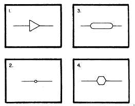
3-24. Which of the following symbols
represents an inverter?