3-23
PULSE DEMODULATION
Pulse modulation is used in radar circuits as well as communications circuits, as discussed in chapter
2. A pulse-modulated signal in radar may be detected by a simple circuit that detects the presence of rf
energy. Circuits that are capable of this were covered in this chapter in the cw detection discussion;
therefore, the information will not be repeated here. A RADAR DETECTOR, in its simplest form, must
be capable of producing an output when rf energy (reflected from a target) is present at its input.
In COMMUNICATIONS PULSE DETECTORS the modulated waveform must be restored to its
original form. In this chapter you will study three basic methods of pulse demodulation: PEAK,
LOW-PASS FILTER, and CONVERSION.
PEAK DETECTION
Peak detection uses the amplitude of a pulse-amplitude modulated (pam) signal or the duration of a
pulse-duration modulated (pdm) signal to charge a holding capacitor and restore the original waveform.
This demodulated waveform will contain some distortion because the output wave is not a pure sine
wave. However, this distortion is not serious enough to prevent the use of peak detection.
Pulse-Amplitude Demodulation
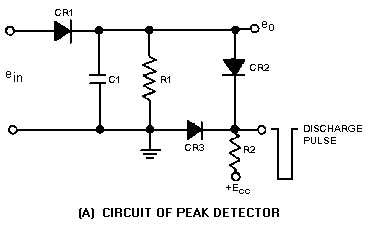
Peak detection is used to detect pam. Figure 3-21 includes a simplified circuit [view (A)] for this
demodulator and its waveforms [views (B) and (C)]. CR1 is the input diode which allows capacitor C1 to
charge to the peak value of the pam input pulse. Pam input pulses are shown in view (B). CR1 is reverse
biased between input pulses to isolate the detector circuit from the input. CR2 and CR3 are biased so that
they are normally nonconducting. The discharge path for the capacitor is through the resistor (R1). These
components are chosen so that their time constant is at least 10 times the interpulse period (time between
pulses). This maintains the charge on C1 between pulses by allowing only a small discharge before the
next pulse is applied. The capacitor is discharged just prior to each input pulse to allow the output voltage
to follow the peak value of the input pulses. This discharge is through CR2 and CR3. These diodes are
turned on by a negative pulse from a source that is time-synchronous with the timing-pulse train at the
transmitter. Diode CR3 ensures that the output voltage is near 0 during this discharge period. View (C)
shows the output wave shape from this circuit. The peaks of the output signal follow very closely the
original modulating wave, as shown by the dotted line. With additional filtering this stepped waveform
closely approximates its original shape.
Figure 3-21A.—Peak detector. CIRCUIT OF PEAK DETECTOR.

