3-9
level signals. The next sections will discuss two of these circuits, the common-emitter and common-base
detectors.
Q-13.
How does the current-diode detector differ from the voltage-diode detector?
Q-14.
Under what circuit conditions would the shunt detector be used?
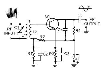
COMMON-EMITTER DETECTOR
The COMMON-EMITTER DETECTOR is often used in receivers to supply an amplified detected
output. The schematic for a typical transistor common-emitter detector is shown in figure 3-7. Input
transformer T1 has a tuned primary that acts as a frequency-selective device. L2 inductively couples the
input modulation envelope to the base of transistor Q1. Resistors R1 and R2 are fixed-bias voltage
dividers that set the bias levels for Q1. Resistor R1 is bypassed by C2 to eliminate rf. This RC
combination also acts as the load for the diode detector (emitter-base junction of Q1). The detected audio
is in series with the biasing voltage and controls collector current. The output is developed across R4
which is also bypassed to remove rf by C4. R3 is a temperature stabilization resistor and C3 bypasses it
for both rf and af.
Figure 3-7.—Common-emitter detector.
Q1 is biased for slight conduction with no input signal applied. When an input signal appears on the
base of Q1, it is rectified by the emitter-base junction (operating as a diode) and is developed across R1 as
a dc bias voltage with a varying af component. This voltage controls bias and collector current for Q1.
The output is developed by collector current flow through R4. Any rf ripple in the output is bypassed
across the collector load resistor by capacitor C4. The af variations are not bypassed. After the modulation
envelope is detected in the base circuit, it is amplified in the output circuit to provide suitable af output.
The output of this circuit is higher than is possible with a simple detector. Because of the amplification in
this circuit, weaker signals can be detected than with a simple detector. A higher, more usable output is
thus developed.
Q-15.
Which junction of the transistor in the common-emitter detector detects the modulation
envelope?
Q-16.
Which component in figure 3-7 develops the af signal at the input?
Q-17.
How is the output signal developed in the common-emitter detector?