3-45
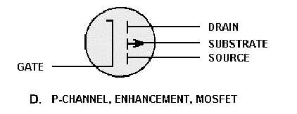
Figure 3-52D.—MOSFET symbols.
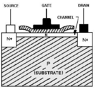
The construction of an N-channel MOSFET is shown in figure 3-53. Heavily doped N-type regions
(indicated by the N+) are diffused into a P-type substrate or base. A channel of regular N-type material is
diffused between the heavily doped N-type regions. A metal oxide insulating layer is then formed over
the channel, and a metal gate layer is deposited over the insulating layer. There is no electrical connection
between the gate and the rest of the device. This construction method results in the extremely high input
impedance of the MOSFET. Another common name for the device, derived from the construction
method, is the insulated gate field effect transistor (IGFET).
Figure 3-53.—MOSFET structure.
The operation of the MOSFET, or IGFET, is basically the same as the operation of the JFET. The
current flow between the source and drain can be controlled by using either of two methods or by using a
combination of the two methods. In one method the drain voltage controls the current when the gate
potential is at zero volts. A voltage is applied to the gate in the second method. An electric field is formed
by the gate voltage that affects the current flow in the channel by either depleting or enhancing the
number of current carriers available. As previously stated, a reverse bias applied to the gate depletes the
carriers, and a forward bias enhances the carriers. The polarity of the voltages required to forward or
reverse bias a MOSFET depends upon whether it is of the P-channel type or the N-channel type. The
effects of reverse-bias voltage on a MOSFET designed to operate in the depletion mode are illustrated in