3-43
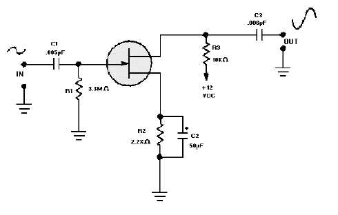
Figure 3-51 shows a basic common-source amplifier circuit containing an N-channel JFET. The
characteristics of this circuit include high input impedance and a high voltage gain. The function of the
circuit components in this figure is very similar to those in a triode vacuum tube common-cathode
amplifier circuit. C1 and C3 are the input and output coupling capacitors. R1 is the gate return resistor and
functions much like the grid return resistor in a vacuum tube circuit. It prevents unwanted charge buildup
on the gate by providing a discharge path for C1. R2 and C2 provide source self-bias for the JFET, which
operates like cathode self-bias. R3 is the drain load resistor, which acts like the plate or collector load
resistor.
Figure 3-51.—JFET common source amplifier.
The phase shift of 180 degrees between input and output signals is the same as that of common-
cathode vacuum tube circuits (and common-emitter transistor circuits). The reason for the phase shift can
be seen easily by observing the operation of the N-channel JFET. On the positive alternation of the input
signal, the amount of reverse bias on the P-type gate material is reduced, thus increasing the effective
cross-sectional area of the channel and decreasing source-to-drain resistance. When resistance decreases,
current flow through the JFET increases. This increase causes the voltage drop across R3 to increase,
which in turn causes the drain voltage to decrease. On the negative alternation of the cycle, the amount of
reverse bias on the gate of the JFET is increased and the action of the circuit is reversed. The result is an
output signal, which is an amplified 180-degree-out-of-phase version of the input signal.
A second type of field-effect transistor has been introduced in recent years that has some advantages
over the JFET. This device is the metal oxide semiconductor field effect transistor (MOSFET). The
MOSFET has an even higher input impedance than the JFET (10 to 100 million megohms). Therefore,
the MOSFET is even less of a load on preceding circuits. The extremely high input impedance, combined
with a high gain factor, makes the MOSFET a highly efficient input device for RF/IF amplifiers and
mixers and for many types of test equipment.
The MOSFET is normally constructed so that it operates in one of two basic modes: the depletion
mode or the enhancement mode. The depletion mode MOSFET has a heavily doped channel and uses
reverse bias on the gate to cause a depletion of current carriers in the channel. The JFET also operates in
this manner. The enhancement mode MOSFET has a lightly doped channel and uses forward bias to