1-37
allow greater wiring density on boards
Figure 1-39 illustrates how individual boards are mated to form the multilayer unit. Although all
multilayer boards are similarly constructed, various methods can be used to interconnect the circuitry
from layer to layer. Three proven processes are the clearance-hole, plated-through hole, and layer build-
up methods.
Figure 1-39.—Multilayer pcb.
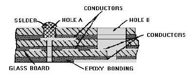
CLEARANCE-HOLE METHOD.—In the CLEARANCE-HOLE method, a hole is drilled in the
copper island (terminating end) of the appropriate conductor on the top layer. This provides access to a
conductor on the second layer as shown by hole A in figure 1-40. The clearance hole is filled with solder
to complete the connection. Usually, the hole is drilled through the entire assembly at the connection site.
This small hole is necessary for the SOLDER-FLOW PROCESS used with this interconnection method.
Figure 1-40.—Clearance-hole interconnection.


