2-6
TRANSISTOR THEORY
You should recall from an earlier discussion that a forward-biased PN junction is comparable to a low-
resistance circuit element because it passes a high current for a given voltage. In turn, a reverse-biased PN
junction is comparable to a high-resistance circuit element. By using the Ohm's law formula for power
(P = I2R) and assuming current is held constant, you can conclude that the power developed across a high
resistance is greater than that developed across a low resistance. Thus, if a crystal were to contain two PN
junctions (one forward-biased and the other reverse-biased), a low-power signal could be injected into the
forward-biased junction and produce a high-power signal at the reverse-biased junction. In this manner, a
power gain would be obtained across the crystal. This concept, which is merely an extension of the material
covered in chapter 1, is the basic theory behind how the transistor amplifies. With this information fresh in
your mind, let's proceed directly to the NPN transistor.
NPN Transistor Operation
Just as in the case of the PN junction diode, the N material comprising the two end sections of the NP N
transistor contains a number of free electrons, while the center P section contains an excess number of holes.
The action at each junction between these sections is the same as that previously described for the diode;
that is, depletion regions develop and the junction barrier appears. To use the transistor as an amplifier, each
of these junctions must be modified by some external bias voltage. For the transistor to function in this
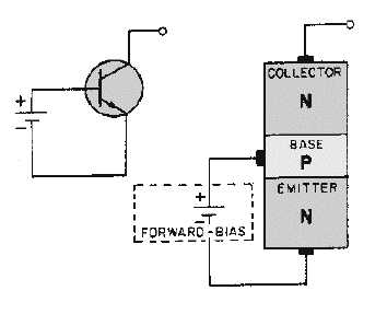
capacity, the first PN junction (emitter-base junction) is biased in the forward, or low-resistance, direction.
At the same time the second PN junction (base-collector junction) is biased in the reverse, or high-
resistance, direction. A simple way to remember how to properly bias a transistor is to observe the NPN or
PNP elements that make up the transistor. The letters of these elements indicate what polarity voltage to use
for correct bias. For instance, notice the NPN transistor below:
1. The emitter, which is the first letter in the NPN sequence, is connected to the negative side of the
battery while the base, which is the second letter (NPN), is connected to the positive side.
2. However, since the second PN junction is required to be reverse biased for proper transistor
operation, the collector must be connected to an opposite polarity voltage (positive) than that
indicated by its letter designation(NPN). The voltage on the collector must also be more positive
than the base, as shown below:


