3-49
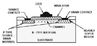
Figure 3-56.—Induced channel MOSFET construction.
The induced-channel MOSFET is caused to conduct from source to drain by the electric field that is
created when a voltage is applied to the gate. For example, assume that a negative voltage is applied to
the MOSFET in figure 3-56. The effect of the negative voltage modifies the conditions in the substrate
material. As the gate builds a negative charge, free electrons are repelled, forming a depletion region.
Once a certain level of depletion has occurred (determined by the composition of the substrate material),
any additional gate bias attracts positive holes to the surface of the substrate. When enough holes have
accumulated at the surface channel area, the channel changes from an N-type material to a P-type
material, since it now has more positive carriers than negative carriers. At this point the channel is
considered to be to inverted, and the two P-type regions at the source and the drain are now connected by
a P-type inversion layer or channel. As with the MOSFET, the gate signal determines the amount of
current flow through the channel as long as the source and drain voltages remain constant. When the gate
voltage is at zero, essentially no current flows since a gate voltage is required to form a channel.
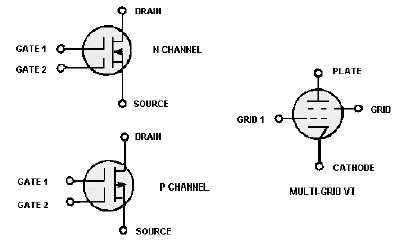
The MOSFETs discussed up to this point have been single-gate MOSFETs. Another type of
MOSFET, the dual-gate type, is shown in figure 3-57. As the figure shows, the gates in a dual-gate
MOSFET can be compared to the grids in a multi-grid vacuum tube. Because the substrate has been
connected directly to the source terminal, the dual-gate MOSFET still has only four leads: one each for
source and drain, and two for the gates. Either gate can control conduction independently, making this
type of MOSFET a truly versatile device.
Figure 3-57.—Dual-gate MOSFET.