2-17
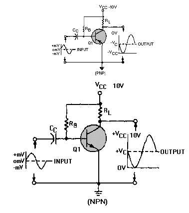
Figure 2-12.—The basic transistor amplifier.
With Q1 properly biased, direct current flows continuously, with or without an input signal, throughout
the entire circuit. The direct current flowing through the circuit develops more than just base bias; it also
develops the collector voltage (VC) as it flows through Q1 and R
L. Notice the collector voltage on the output
graph. Since it is present in the circuit without an input signal, the output signal starts at the VC level and
either increases or decreases. These dc voltages and currents that exist in the circuit before the application of
a signal are known as QUIESCENT voltages and currents (the quiescent state of the circuit).
Resistor RL, the collector load resistor, is placed in the circuit to keep the full effect of the collector
supply voltage off the collector. This permits the collector voltage (VC) to change with an input signal,
which in turn allows the transistor to amplify voltage. Without RL in the circuit, the voltage on the collector
would always be equal to VCC.
The coupling capacitor (CC) is another new addition to the transistor circuit. It is used to pass the ac
input signal and block the dc voltage from the preceding circuit. This prevents dc in the circuitry on the left
of the coupling capacitor from affecting the bias on Q1. The coupling capacitor also blocks the bias of Q1
from reaching the input signal source.
The input to the amplifier is a sine wave that varies a few millivolts above and below zero. It is
introduced into the circuit by the coupling capacitor and is applied between the base and emitter. As the
input signal goes positive, the voltage across the emitter-base junction becomes more positive. This in effect
increases forward bias, which causes base current to increase at the same rate as that of the input sine wave.
Emitter and collector currents also increase but much more than the base current. With an increase in
collector current, more voltage is developed across R
L. Since the voltage across RL and the voltage across
Q1 (collector to emitter) must add up to VCC, an increase in voltage across RL results in an equal decrease in


