1-35
maintenance you can replace the faulty module with a good one. The faulty module can then be repaired
at a later time or discarded. This concept significantly reduces the time equipment is inoperable.
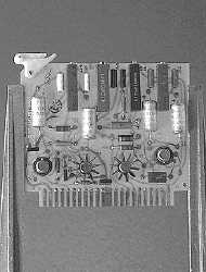
Figure 1-37.—Printed circuit board (pcb).
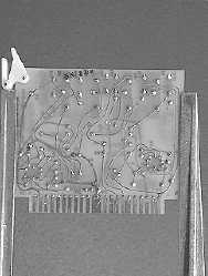
LEVEL II.—Level II packaging is composed of large printed circuit boards and/or cards (mother
boards). Typical units of this level are shown in figures 1-37 and 1-38. In figure 1-38 the card measures
15
5.25 inches. The large dual inline packages (DIPs) are 2.25 inches x 0.75 inch. Other DIPs on the
pcb are much smaller. Interconnections are shown between DIPs. You should also be able to locate a few
discrete components. Repair consists of removing the faulty DIP or discrete component from the pcb and
replacing it with a new part. Then the pcb is placed back into service. The removed part may be a level 0
or I part and would be handled as described in those sections. In some cases, the entire pcb should be
replaced.
Figure 1-38.—Printed circuit board (pcb).