2-15
Inputs X and Y are applied to the AND gate. If either X or Y or both are LOW (view A), then the
output of the AND gate is LOW. A LOW (logic 0) on the input of the inverter results in a HIGH (logic 1)
output. When both X and Y are HIGH (view B), the output of the AND gate is HIGH; thus the output of
the inverter is LOW. The Boolean expression for the output of a NAND gate with these inputs is f = XY .
The expression is spoken "X AND Y quantity NOT." The output of any NAND gate is the negation of the
input. For example, if our inputs are X and Y , the output will be
Y
X
.
NAND GATE OPERATION
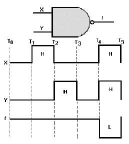
Now, let’s observe the logic level inputs and corresponding outputs as shown in figure 2-13. At time
T0, X and Y are both LOW. The output is HIGH; the opposite of an AND gate with the same inputs. At
T1, X goes HIGH and Y remains LOW. As a result, the output remains HIGH. At T2, X goes LOW and Y
goes HIGH. Again, the output remains HIGH. When both X and Y are HIGH at T4, the output goes LOW.
The output will remain LOW only as long as both X and Y are HIGH.
Figure 2-13. —NAND gate input and output signals.
TRUTH TABLE
The Truth Table for a NAND gate with X and Y as inputs is shown below.
X
Y
f
0
0
1
0
1
1
1
0
1
1
1
0
F = XY
Q16. A NAND gate has Z and X as inputs. What will be the output logic level if Z is HIGH and X is
LOW?
Q17. What must be the state of the inputs to a NAND gate in order to produce a LOW output?


