2-10
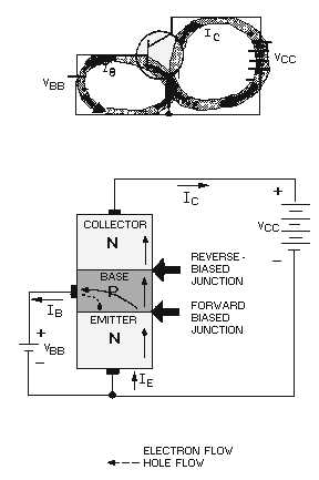
Figure 2-7.—NPN transistor operation.
The bias batteries in this figure have been labeled V
CC
for the collector voltage supply, and VBB for the
base voltage supply. Also notice the base supply battery is quite small, as indicated by the number of cells in
the battery, usually 1 volt or less. However, the collector supply is generally much higher than the base
supply, normally around 6 volts. As you will see later, this difference in supply voltages is necessary to have
current flow from the emitter to the collector.
As stated earlier, the current flow in the external circuit is always due to the movement of free
electrons. Therefore, electrons flow from the negative terminals of the supply batteries to the N-type emitter.
This combined movement of electrons is known as emitter current (IE). Since electrons are the majority
carriers in the N material, they will move through the N material emitter to the emitter-base junction. With
this junction forward biased, electrons continue on into the base region. Once the electrons are in the base,
which is a P-type material, they become minority carriers. Some of the electrons that move into the base
recombine with available holes. For each electron that recombines, another electron moves out through the
base lead as base current IB (creating a new hole for eventual combination) and returns to the base supply
battery V
BB. The electrons that recombine are lost as far as the collector is concerned. Therefore, to make
the transistor more efficient, the base region is made very thin and lightly doped. This reduces the
opportunity for an electron to recombine with a hole and be lost. Thus, most of the electrons that move into
the base region come under the influence of the large collector reverse bias. This bias acts as forward bias
for the minority carriers (electrons) in the base and, as such, accelerates them through the base-collector
junction and on into the collector region. Since the collector is made of an N-type material, the electrons that
reach the collector again become majority current carriers. Once in the collector, the electrons move easily
through the N material and return to the positive terminal of the collector supply battery VCC as collector
current (IC).