1-16
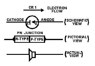
Figure 1-12.—The PN junction diode.
CONSTRUCTION
Merely pressing together a section of P material and a section of N material, however, is not
sufficient to produce a rectifying junction. The semiconductor should be in one piece to form a proper PN
junction, but divided into a P-type impurity region and an N-type impurity region. This can be done in
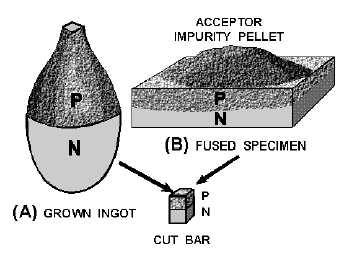
various ways. One way is to mix P-type and N-type impurities into a single crystal during the
manufacturing process. By so doing, a P-region is grown over part of a semiconductor’s length and N-
region is grown over the other part. This is called a GROWN junction and is illustrated in view A of
figure 1-13. Another way to produce a PN junction is to melt one type of impurity into a semiconductor
of the opposite type impurity. For example, a pellet of acceptor impurity is placed on a wafer of N-type
germanium and heated. Under controlled temperature conditions, the acceptor impurity fuses into the
wafer to form a P-region within it, as shown in view B of figure 1-13. This type of junction is known as
an ALLOY or FUSED-ALLOY junction, and is one of the most commonly used junctions. In figure 1-14,
a POINT-CONTACT type of construction is shown. It consists of a fine metal wire, called a cat whisker,
that makes contact with a small area on the surface of an N-type semiconductor as shown in view A of the
figure. The PN union is formed in this process by momentarily applying a high-surge current to the wire
and the N-type semiconductor. The heat generated by this current converts the material nearest the point
of contact to a P-type material (view B).
Figure 1-13.—Grown and fused PN junctions from which bars are cut.