3-41
"depletion region" to form around the PN junction of the JFET. Because this region has a reduced number
of current carriers, the effect of reverse biasing is to reduce the effective cross-sectional area of the
"channel." This reduction in area increases the source-to-drain resistance of the device and decreases
current flow.
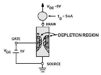
Figure 3-48.—JFET with reverse bias.
The application of a large enough negative voltage to the gate will cause the depletion region to
become so large that conduction of current through the bar stops altogether. The voltage required to
reduce drain current (ID) to zero is called "pinch-off" voltage and is comparable to "cut-off" voltage in a
vacuum tube. In figure 3-48, the negative 1 volt applied, although not large enough to completely stop
conduction, has caused the drain current to decrease markedly (from 10 milliamperes under zero gate bias
conditions to 5 milliamperes). Calculation shows that the 1-volt gate bias has also increased the resistance
of the JFET (from 500 ohms to 1 kilohm). In other words, a 1-volt change in gate voltage has doubled the
resistance of the device and cut current flow in half.
These measurements, however, show only that a JFET operates in a manner similar to a bipolar
transistor, even though the two are constructed differently. As stated before, the main advantage of an
FET is that its input impedance is significantly higher than that of a bipolar transistor. The higher input
impedance of the JFET under reverse gate bias conditions can be seen by connecting a microammeter in
series with the gate-source voltage (V
GG), as shown in figure 3-49.